Terahertz electronics and photonics
Facilities
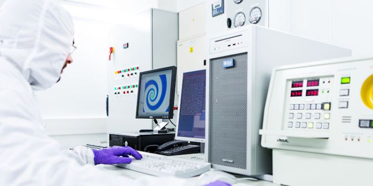
The Terahertz Electronics and Photonics group benefit from extensive facilities in purpose-built laboratories, including:
- Eight optical bench based systems, with five femtosecond pulsed imaging and spectroscopy systems, including ultra-broadband (>20THz), pump-probe, and both free-space and guided-wave apparatus.
- A Bruker 66v Fourier transform infrared spectrometer, and QCL-based imaging and spectroscopy systems, in both transmission and reflection geometries (specular and diffuse), including self-mixing interferometry.
- An 8mK cryogen-free dilution refrigerator, with fibre-optic and microwave access, several 1.2K optical access cryostats, including cryogen-free systems, and magnetic fields up to 12T.
Researchers also benefit from two state-of-the-art MBE growth chambers, focused on III-V semiconductors for terahertz devices; a nanotechnology fabrication facility, including deposition, etching, bonding and packaging; and the regional JEOL Electron Beam Lithography facility, enabling wafer-scale patterning to sub-10 nm resolution.
Extensive software is also available for modelling semiconductor band structures, waveguides, laser dynamics, and THz vibrational modes (including High Performance Computing (HPC)).