Condensed Matter
Facilities

We are developing our research portfolio to focus on these aspects, and this is reflected in our extensive suite of facilities.
Materials growth
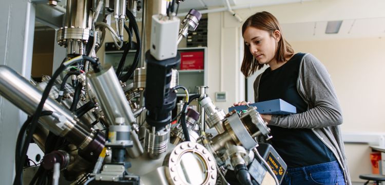
We have world-class facilities for the deposition of thin films including metals, oxides and semiconductors. In particular, we specialise in the growth of magnetic multilayers for spintronic applications. The thin films are grown via physical vapour deposition (PVD) processes namely sputtering, molecular beam epitaxy and evaporation. In addition to PVD we also produce layers of organic materials including C60 and epitaxial graphene.
Fabrication
We make use of the University's Wolfson cleanrooms that are located in the School of Electronic and Electrical Engineering. The cleanroom has facilities for photolithography, electron-beam lithography and focused-ion-beam lithography as well as standard wet and dry etching processes. In addition, we have a Nanoprobe system containing an SEM column and four scanning probe tips.
Sample characterisation
The samples produced in the group require sophisticated measurement techniques. We determine the electrical, structural and magnetic properties of our samples over a range of temperatures and magnetic fields. We utilise a range of facilities related to transport measurements, magnetometry, structural characterisation and microscopy.

