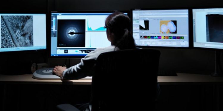
Leeds electron microscopy and spectroscopy centre
- Overview: LEMAS is part of the Bragg Centre for Materials Research and is jointly run by the Faculty of Engineering and Physical Sciences and the School of Earth & Environment at Leeds. It aims to develop and underpin Imaging and characterisation techniques for the examination of the morphology, structure and chemical composition of Advanced Materials, including soft materials, drawn from the physical, engineering and geosciences.
- Contact name: John Harrington, Facility Manager
- Phone: +44 (0)113 343 2559
- Email: j.p.harrington@leeds.ac.uk

Specialist technologies include:
- High spatial resolution microanalysis
- Light element composition and chemical state information
- Low dose microscopy and spectroscopy
- Analysis of dynamic systems including solid/liquid systems
Equipment
Transmission electron microscopy
- TESCAN Tensor: The world’s first integrated, precession-assisted, 100 kV analytical 4D-STEM fitted with BF, ADF and HAADF, integrated direct electron detector (Dectris Quadro), EDS detectors. Offering imaging, virtual STEM composition, orientation, phase and strain mapping and tomography.
- FEI Titan3 Themis 300: X-FEG 300 kV S/TEM with S-TWIN objective lens, monochromator (energy spread approx. 0.25 eV), multiple HAADF/ADF/BF STEM detectors, FEI Super-X 4-detector EDX system, Gatan Quantum ER energy filter for EELS and EFTEM and Gatan OneView 4K CMOS digital camera.
Dual beam FIBSEM
- Tescan AmberX Plasma FIBSEM: Combination of high throughput, large area Plasma FIB and field-free UHR FEGSEM for multiscale materials characterization including Oxford Instruments Aztec Energy EDX system with EBSD, integrated time of flight secondary ion mass spectrometer – ToFSIMS and Quorum PP3010T Cryo SEM capabilities. 3D Large Volume Microscopy.
- FEI Helios G4 CX DualBeam: High resolution monochromated FEGSEM with precise Focused Ion Beam (FIB).
- In-situ TEM sample preparation and Slice&View acquisition of multi signal 3D data sets.
Scanning electron microscopy
- Hitachi SU8230: High-performance cold-field emission (CFE) SEM with Oxford Instruments Aztec Energy EDX system with 80mm X-Max SDD detector - Ultra high resolution, low kV, Simultaneous SE, BSE, BF and DF imaging, with nanoscale resolution as well as nanoscale EDX capabilities.
- Carl Zeiss EVO MA15: Variable pressure W SEM with Oxford Instruments AZtecEnergy EDX system with 80mm X-Max SDD detector- secondary and backscattered imaging, EDX elemental mapping and linescans plus CZ STEM detector.
- FEI Quanta 650: FEGESEM environmental SEM with Oxford Instruments INCA 350 EDX system/80mm X-Max SDD detector, EBSD and KE Centaurus EBSD system.SEM for orientation imaging, texture analysis etc with environmental capabilities.
- Jeol 8230: Dedicated electron microprobe with 5 spectrometers, EDS/EDX capabilities- for quantitative mapping and microanalysis.
- Tescan VEGA3 XM: Tungsten source machine with large chamber and high sample throughput, equipped with X-max 150 SDD EDS and Aztec 3.3 software, also RGB filtered CL system.
Applications
Characterising the morphology, structure, and chemical composition of hard and soft materials from atomic to microstructural length scales is vital in understanding a material’s physical and chemical behaviour. This analysis lies at the interface between physics and engineering and has enabled significant improvements both to traditional materials and the development of entirely new materials for specific applications.
Specialist research areas:
- Metals, semiconductors, and ceramics
- Functional materials and coatings
- Nanoparticles and nanomaterials
- Biomaterials
- Soft materials
- Composite materials and formulations
- Porous materials
Who can use the facility?
We aim to develop and underpin materials characterisation techniques at the University of Leeds and to also offer external services to outside higher education institutions and industry.

