Molecular beam epitaxy facility
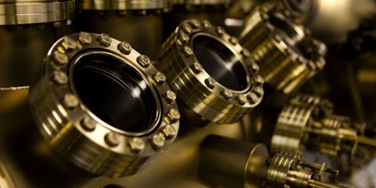
- Overview: Our in-house Oxford Instruments V80H III–V MBE machine gives us the ability to grow layered compound semiconductor structures
- Contact name: Professor Edmund Linfield
- Phone: +44(0)113 343 2015
- Email: e.h.linfield@leeds.ac.uk
Molecular beam epitaxy (MBE) is a flexible technique used to grow layered compound semiconductor structures of extremely high purity and with atomic-scale resolution of composition and doping in the growth direction.
This technique has been central to a number of electronic, optoelectronic and nanotechnology developments over the past 20 years. These include the growth and development of mid- and far-infrared (terahertz) quantum cascade lasers and the fabrication of advanced materials such as low-temperature gallium arsenide and related compounds used for optical mixers and electro-optic switches.
Our in-house Oxford Instruments V80H III–V MBE machine and facility gives us a competitive advantage in the fields of condensed matter physics, terahertz electronics and photonics, optoelectronics, semiconductor materials, semiconductor device engineering, photonics and nanotechnology.
We supply material and devices to researchers in the UK and internationally. The quality of the material growth is evidenced by our extensive research collaborations with the universities of Harvard, Paris-VII, Paris-South, Georgia Tech, Vilnius and Frankfurt, among others.
Who can use the facility?
We are committed to sharing our facilities and associated expertise with external academic and industrial collaborators. To make an enquiry please email Professor Edmund Linfield, e: e.h.linfield@leeds.ac.uk